
? We all know about hard disk drives (HDDs). They’re mechanical, have spindles, and use read/write heads that float over magnetic coated discs spinning at 5,400 or 7,200 RPM. We also know that their moving mechanical parts wear out over time. Although technology and HDD controllers have certainly improved since their introduction by IBM in 1956, the basic technology has been around nearly 60 years!1 However, for several years now, there has been an alternative: solid state drives (SSDs).
Will SSDs ever totally replace hard disk drives? Other than cost, SSDs have everything going for them. At the top of the list: There are no mechanical parts to wear out. This also means SSDs are quiet, more physically robust, much smaller, and more power-efficient. Their biggest advantage is ultrafast data transfers while maintaining random accessibility.
SSD on-chip densities are also getting higher. For example, last year Intel announced that in addition to building chips on 14-nm technology, it will be shipping 10-nm chips in 2015, followed by 7-nm technology in 2017. This will mean higher densities and more memory in smaller, less power-hungry formats for lower cost.2 (It can be difficult to imagine how small a nanometer really is. For comparison, if the earth represented a meter, a nm would be the size of a marble.3)
In this, part one of a two-part series in “Networking,” we’ll explore flash memory and SSD structures. Next month, in part 2, our focus will shift to exploring the key differences between SSD and HDD technologies, with a few buying tips along the way.
A Brief History
Rather than retracing the entire history of memory chips, I’ll only go as far back as EPROMs. Some readers will remember when the nonvolatile memory came in a programmable package called an Erasable Programmable Read Only Memory, or EPROM. It had a round window on the top of the integrated circuit where you could see the memory chip inside. You could reprogram the EPROM by shining UV light into the window to erase the memory. The only choice was to erase the entire memory.
A special fixture was required that would apply the right programming voltages to allow the new information or program to be burned in. Once programmed, a paper label identifying the contents was applied over the chip window.
I recall when a fellow tech came to me and asked, “What does it mean when the LED comes on in the EPROM?” “LED?” I thought. “There’s no LED in there.” Then I saw what he was talking about. The chip inside was glowing red hot, and the paper label had already burned off. It turns out that he had plugged it in backward. So I said, “Oh, when the red LED comes on, it means you’ve plugged it in backward and need to throw it away—after it cools down!”
The next generation was an electrically erasable PROM (EEPROM or E2PROM). This could be programmed in-circuit by applying a much lower voltage to the programming pins on the integrated circuit (IC). Although you still had to wipe it clean and program the entire memory each time, you no longer needed UV lights and a special programming fixture.
These types of ICs are also called firmware when used as nonvolatile memory for system boot-up purposes. For example, in PCs, the firmware is needed for boot-up and has code for elementary basic function to provide services to higher-level software like the operating system. A CATV remote control uses firmware for the entire application, and a basic operating system is needed to provide operation of the remote. Firmware these days will most likely be flash memory, which was developed from EEPROM technology.
How Flash Works
Flash is also nonvolatile and comes in two types: NAND and NOR. You no longer need to erase the entire chip to be able to write to it. Taking better advantage of the random accessibility, NAND memory allows the rewriting of certain blocks or pages of memory. Flash memory cells are grouped into pages. Pages are organized into blocks. Read/write (R/W) operations are page oriented in NAND technology, while erase operations happen at the block level.
NOR memory allows single machine word or byte-level access, and its ultrafast accessibility is best used as L1 or L2 CPU cache memory. NOR technology is more expensive to manufacture than NAND, so it is not used for much other than processor cache. NAND-type flash is typically the media used in SSD and USB memory sticks as the most prevalent form of flash. NAND also has a common ground interconnect for all the transistors, which allows a higher density than NOR. NOR has a separate ground interconnect for each transistor, and since the interconnects are physically large by comparison, they take up a lot of on-chip space.
The term flash comes from the Japanese inventors who thought the voltage flash for reprogramming the memory reminded them of a camera flash. The term stuck. Flash memory is based on floating gate transistors (see Figure 1). There are oxide layers that keep the added floating gate electrically isolated. When a strong-enough voltage is applied across the control gate and source connections, the oxide layer allows electron migration into (write) or out of (read) the floating gate, depending on the voltage applied.
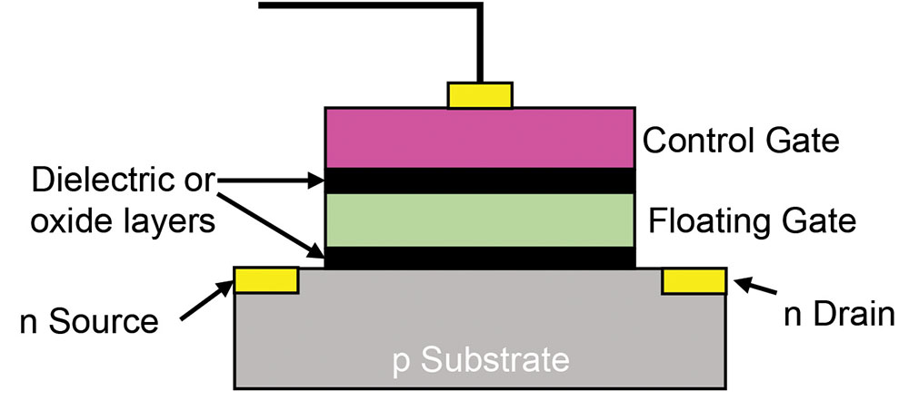
Figure 1: The floating gate transistor. (Click image to Enlarge.)
The charge can stay in the isolated floating gate for years. When there’s a negative charge stored, it is labeled as storing a digital 0. If there is no charge, it is a digital 1. A good way to remember this is to picture that 0 V is higher than a negative voltage. Therefore, 0 V is a 1 and a negative, lower voltage represents a 0.
To read a NAND gate, a read-level voltage is applied across the control gate and source connection to check for current flow. If there is no current flow—because the floating gate is empty—it must be storing a digital 1. If there is current flow, it must be because the floating gate is full of stored electrons, allowing a path for the current to flow, so it must be storing a digital 0.4
The Flash Durability Issue
Over time, with many read/erase/write cycles, the oxide layer starts to degrade from spurious electrons that are cast off during a read, erase, or write operation. Is this a cause for worry? I think too much is made of degradation. It’s related to how many R/W cycles the transistors can handle before the oxide layer degrades to a point where the memory cell becomes unreliable. The maximum number of these program/erase (P/E) cycles can be as low as 2,500.
Intel rates its flash memory based on 10 GB being erased and rewritten every 24 hours for 365 days. This equates to about 22 total P/E cycles per year. So 2,500 cycles divided by 22 cycles per year works out to 113 years. Even at more than twice this rate (48 cycles per year), it’s still a 52-year life span.5
Will SSDs degrade and wear out? The answer is yes, but their life span appears to be much longer than the HDD’s mechanical life span—and maybe even our own life span! The memory sticks you’ve been using for the past 10 years only have about 40 years left—better start copying that stuff to DVDs for longer storage. Hopefully, people in the future will have access to DVD drives to read the information, assuming that the DVD doesn’t degrade as fast as an SSD.
Memory Cell Structure
You will also see acronyms related to flash memory when in the market for a SSD: SLC, MLC, and TLC (see Figure 2). They reflect how the chip is built and have implications for data and power consumption. Single-level cells (SLCs) have one floating gate transistor in each memory cell, and therefore can store one bit—a 1 or a 0. Multilevel cells (MLCs) can have more than one, but most often have just two transistors per cell, and therefore can store 2 bits as 00, 01, 10, or 11. Triple-level cells (TLCs) have three transistors per cell, and therefore can store three bits as 000, 001, 010, 011, 100, 101, or 111.6
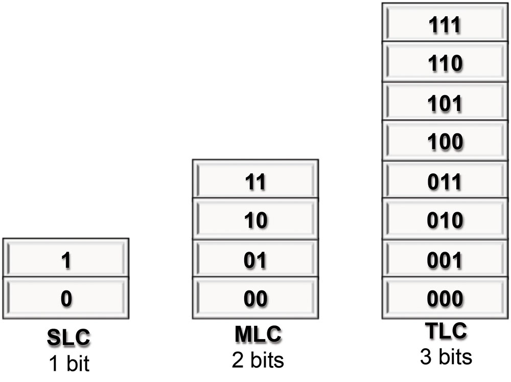
Figure 2: Flash cell memory structure. (Click image to enlarge.)
In general, SLC is the most stable and reliable type, but also the most expensive per gigabyte. MLC doubles the level of storage, resulting in lower cost than SLC. MLC is the most common in consumer devices like USB memory sticks. For the same reason, TLC is the least expensive per gigabyte of storage. However, TLC has the most transistors jammed into a cell. More transistors means more wayward electrons bouncing around the cell during P/E cycles. This makes the TLC the least reliable type, as it tends to break down the oxide layers a bit faster.
These types of flash memory also have different P/E cycles or life spans. For TLC and MLC, typical maximum P/E cycles range from 1,500 to 10,000. For SLC, devices can execute up to roughly 100,000 P/E cycles.5
Conclusion
The construction of the memory has much to do with making it operate ultrafast while keeping it reliable. However, the speed of the data transfer also depends upon the controllers and applications that move data in and out of memory.
In part 2, we’ll look at the methods used to get the most out of flash speeds. We’ll also compare HDDs and SSDs more directly and also look at what you should know when going about purchasing SSDs. 24×7
Jeff Kabachinski is the director of technical development for Aramark Healthcare Technologies in Charlotte, NC. For more information, contact [email protected].
References
1. Baxter A. (2014). SSD vs HDD. Retrieved from StorageReview.com: http://www.storagereview.com/ssd_vs_hdd. Accessed November 7, 2014.
2. Mujtaba H. (2014, October 29). IDF13: Intel Showcases 14nm Broadwell CPU Powered Laptop and Haswell-Y – Broadwell Chips To Ship By End of 2013. Retrieved from WCCF Tech: http://wccftech.com/idf13-intel-showcases-14nm-broadwell-cpu-powered-laptop-haswelly-broadwell-chips-ship-2013/. Accessed November 7, 2014.
3. Newton H. Newton’s Telecomm Dictionary. New York: Flat Iron Publishing; 2011.
4. Wikipedia. (2014, November 1). Flash Memory. Retrieved from Wikipedia: https://en.wikipedia.org/wiki/NAND_flash#NAND_memories. Accessed November 7, 2014.
5. Hagedoorn H. (2013, August 15). Intel 530 SSD review – What is SATA 3 (6G) ? – 1x nm NAND – MLC . Retrieved from The Guru of 3D: http://www.guru3d.com/articles-pages/intel-530-ssd-benchmark-review-test,3.html. Accessed November 7, 2014.


thank you for the timely article comparing traditional hard drives vs. solid state drives, very informative. mechanical hd vs gradual degradation of ss