By John Noblitt, MAEd, CBET
 Many HTM professionals who take the certification exam will tell you their lowest scores came on the electronics section. The reason for this, I believe, is that the exam still has component-level electronic questions, but for various reasons, many technicians and shops are no longer troubleshooting faults to the component level. So this month, to help you in your certification quest, let us take another look at electronics topics.
In previous articles, I have written about basic electronic theory such as Kirchhoff’s laws, which expand on Georg Ohm’s generalized laws of the relationship of resistance, current, and voltage. This information will be extremely important to anyone who seeks certification, since it is used to evaluate electronic circuit operations. In this article I will move on to JFETs, MOSFETs, and some similarities to bipolar transistors.
In electronics we refer to junction field-effect transistors, or JFETs, as unipolar devices because their operation relies on one type of charge. Depending on your preference, it relies on either free electron flow or hole flow. You may relate these concepts to conventional flow or electron flow. Conventional flow assumes current flows from positive to negative, while electron flow assumes current flows from negative to positive. It does not matter which type of flow you use as long as you use the same theorem consistently in your analysis of electronic circuits. As my electronics instructor Norm Svee told me, “Ohm had a 50/50 chance, and he blew it.” It wasn’t until science later understood electrons were negatively charged particles that electron flow theory emerged.
Field-effect transistors, or FETs, are similar to bipolar transistors in that they also have three terminals, but instead of an emitter, base, and collector, FETs have a source, gate, and drain. Bipolar transistors are very good at voltage gain, but the FET families of devices are better suited for current gain. Both devices can be used as amplifiers or switches in electronic circuits (think saturation and cut-off for switches), but the FET family can switch from one state to the other more quickly and are smaller in size, so their application in computers is more widespread. This is because there are no minority carriers in JFETs or metal–oxide–semiconductor field-effect transistors (MOSFETs).
Other similarities between bipolar and unipolar transistors are the supply voltages. In bipolar devices, we have the base supply or VBB, and the collector supply voltages, or VCC. In the FET family, we have VGG or gate supply and VDD or drain supply. JFETs are known as voltage-controlled devices because the gate voltage controls the output current. The gate-to-source voltage, or VGS, determines how much current flows from the source to the drain.
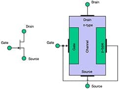
 Figure 1. JFET schematic and construction.
Figure 1 shows a schematic symbol for a JFET on the left and the physical construction of the JFET on the right. With transistors there are PNP and NPN types, and with FETs there are N-channel and P-channel devices. This depends on how the channel is doped. You can determine which type of device you have by the way the gate p-n junction is oriented. In Figure 1, the negative side of the gate diode, or the cathode, is toward the channel, making the device an N-channel JFET.
There are two modes of operations for FETs: depletion mode and enhancement mode. JFETs will always be used in the depletion mode, while MOSFETs can be used in either one. These modes of operation describe whether the device is on or off with 0 VGS. Depletion mode is an ON state and Enhancement mode is an OFF state, given an 0 VGS. Because the JFET is always in the depletion mode and gate current is undesirable, the gate voltage is in reverse bias. We want all the current to flow from source to drain and the gate voltage to control how much current flows in the channel. Given the diagrams in Figure 1 of the N-channel JFET, if we apply a negative voltage to the gate, which is a P material, the channel will become smaller as the negative gate voltage increases. This is no more than a function of the law of charges, which states that like charges repel and opposite charges attract.
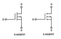
 Figure 2. D- and E-MOSFET schematics.Some technicians may refer to these two modes of operation in the MOSFET as follows: If you move the gate voltage toward the drain voltage, you will enhance the current flow in the channel. If you move the gate voltage away from the drain voltage, you will deplete the channel of current flow. Please note the difference between the schematic symbols in Figure 2 in the D MOSFET and the E MOSFET. Enhancement-mode MOSFETs will always be noted by the broken line in the “channel.” However, both of these two MOSFETs are N-channel devices.
I hope you find this material useful in your journey to become a CBET. We will continue this discussion of electronics when my next column takes a look at thyristors. 24×7
|
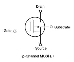
REVIEW QUESTIONS 1) In the MOSFET schematic below, what mode of operation is utilized?
a)Enhancement 2) JFETs will always be used in what mode of operation? 3) FETs are usually used as amplifiers for what? 4) As VGG moves toward VDD, the FET device is said to be more toward which mode of operation? Answers: 1–b; 2–b; 3–c; 4–c.
|
John Noblitt, MAEd, CBET, is the BMET program director at Caldwell Community College and Technical Institute, Hudson, NC. For more information, contact [email protected].


